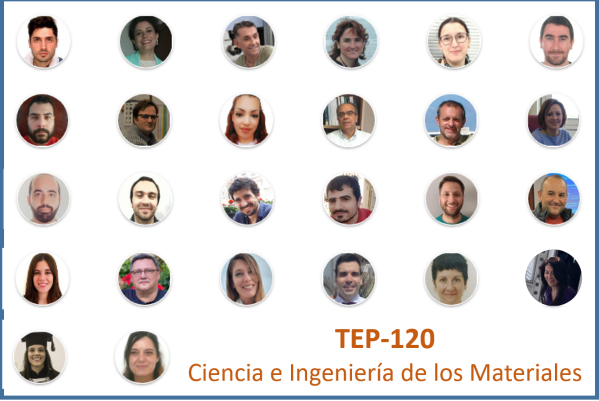
The active research lines focused to specific materials at the CIM-UCA group, at this moment, are:
-Semiconductor nanowires, quantum-wells or quantum-dots for micro- and opto-electronic applications.
-GaAsSbBiN semiconductor alloy engineering for applications in solar cells and high performance photodetectors.
-Multiple systems of thin layers and nanostructures based on the activity of binary III-N nitrides (InN, AlN, GaN), ternary (InAlN, InGaN, AlGaN) and quaternary (InAlGaN) for optoelectronics, power electronics and photovoltaic technology.
-Synthetic diamond for materials engineering in electronics, aeronautics, tools and medicine.
-Systems elaborated by glancing-oblique angle deposition (oxides and metals) for optic, optronic and thermochromic applications.
-Studies of phase transformations of minerals of industrial interest by thermo-chemical treatments.
-Reinforced polymers for aeronautics.
The general objective is to understand relationships between constitutive nature, properties, and methods of synthesis and processing of functional and structural materials; to contribute to the development of their stages of fabrication and implementation, through the elaboration of design rules to accomplish foreseen applications. This is done by (i) micro- and nano-characterization of structure and composition by SEM, FIB, (S)TEM), XRD, etc.; (ii) theoretical-empirical studies and modeling of materials at different scales; (iii) development of new TEM methods and computer simulation of TEM images; (iv) synthesis by CVD and PVD; and (v) electronic and optical characterization.
https://produccioncientifica.uca.es/grupos/7896/colaboracion
On the importance of light scattering for high performances nanostructured antireflective surfaces
Maudet F., Lacroix B., Santos A.J., Paumier F., Paraillous M., Hurand S., Corvisier A., Dupeyrat C., García R., Morales F.M., Girardeau T.
Acta Materialia (2020) Vol: 188. Pgs: 386-393
COMPREHENSIVE (S)TEM CHARACTERIZATION OF POLYCRYSTALLINE GaN/AlN LAYERS GROWN ON LTCC SUBSTRATES.
J.J.Jiménez, J.M. Mánuel, H. Bartsch, J. Breiling, R. García, H.O. Jacobs, J. Müller, J. Pezoldt, F.M. Morales.
Ceramics International. 2019. Vol: 45. Núm: 7. Pgs. 9114-9125.
CONTROL OF NITROGEN INHOMOGENEITIES IN TYPE-I AND TYPE-II GaAsSbN SUPERLATTICES FOR SOLAR CELL DEVICES.
N.Ruiz, V. Braza, A. Gonzalo, D. Fernández, T. Ben, S. Flores, J.M. Ulloa, D. González.
Nanomaterials. 2019. Vol: 9. Núm: 4. Pgs. 623[1]-623[9].
HIGH RESOLUTION BORON CONTENT PROFILOMETRY AT Δ-DOPING EPITAXIAL DIAMOND INTERFACES BY CTEM.
J.C.Piñero, F. Lloret, M.P. Alegre, M.P. Villar, A. Fiori, E. Bustarret, D. Araújo.
Applied Surface Science. 2018. Vol: 461. Pgs. 221-226.
MODELLING OF BISMUTH SEGREGATION IN InAsBi/InAs SUPERLATTICES: DETERMINATION OF THE EXCHANGE ENERGIES.
S.Flores, D.F. Reyes, V. Braza, R.D. Richards, F. Bastiman, T. Ben, N. Ruiz-Marín, J.P.R. David, D. González.
S.Flores, D.F. Reyes, V. Braza, R.D. Richards, F. Bastiman, T. Ben, N. Ruiz-Marín, J.P.R. David, D. González.
